
●目录 章绪论 1.1课题背景和意义 1.2空间辐射环境 1.3逻辑电路的辐射效应 1.3.1单粒子效应和总剂量效应 1.3.2逻辑电路的单粒子效应 1.4国内外研究现状 1.4.1纳米逻辑电路SEU软错误传播规律 1.4.2版图结构对纳米逻辑电路SET影响 1.4.3总剂量效应对纳米逻辑电路SEE影响 1.4.4温度对纳米逻辑电路SEE影响 1.5本书的目标和研究内容 第2章纳米逻辑电路SEU软错误传播规律的研究 2.1本章引论 2.2逻辑电路SEU传播模型分析和仿真验证 2.2.1现有的逻辑电路SEU传播模型分析 2.2.2现有的逻辑电路SEU传播模型仿真验证 2.2.3改进的逻辑电路SEU传播模型 2.3改进的逻辑电路SEU传播模型的实验验证 2.3.1电路设计和实验方法 2.3.2实验结果和讨论 2.4改进的逻辑电路SEU传播模型的应用 2.4.1触发器SEU软错误的加固策略 2.4.2逻辑电路SEE软错误动态截面评估 2.5单粒子软错误传播规律的影响因素 2.5.1电路设计 2.5.2组合逻辑延迟时间的影响 2.5.3入射粒子LET的影响 2.5.4触发器抗SEU性能的影响 2.5.5逻辑电路单粒子软错误截面的预测 2.6本章小结 第3章版图结构对纳米逻辑电路SET影响的研究 3.1本章引论 3.2电路设计和实验方法 3.2.1电路设计 3.2.2实验方法 3.3实验结果和讨论 3.3.1SET脉冲宽度测量精度和测量下限的标定 3.3.2SET脉冲宽度展宽因子的标定 3.3.3重离子垂直入射实验结果和分析 3.3.4重离子斜入射实验结果和分析 3.3.5激光微束单粒子效应实验结果和分析 3.3.6对比分析和讨论 3.4本章小结 第4章总剂量对纳米逻辑电路SEE影响的研究 4.1引言 4.2实验方法 4.3总剂量致静态漏电流变化 4.4总剂量对逻辑电路SEU的影响 4.4.1实验结果 4.4.2实验结果讨论 4.5总剂量对逻辑电路SET的影响 4.5.1实验结果 4.5.2实验结果讨论 4.6本章小结 第5章温度对纳米逻辑电路SEE的影响 5.1引言 5.2电路设计和实验方法 5.2.1电路设计 5.2.2实验方法 5.3温度对逻辑电路SEU的影响 5.3.1实验结果 5.3.2实验结果讨论 5.4温度对逻辑电路SET的影响 5.4.1实验结果 5.4.2实验结果讨论 5.5本章小结 第6章总结与展望 6.1研究总结 6.2本书创新点 6.3需进一步开展的研究 参考文献 在学期间发表的相关学术论文 相关研究成果 致谢 Contents Chapter 1Introduction 1.1Research Background 1.2Radiation Environment in Space 1.3Radiation Effects of Logic Circuit 1.3.1SingleEvent Effect and TID Effect 1.3.2SingleEvent Effect of Logic Circuit 1.4State of the Art of the Research 1.4.1SEU Propagation Principle in NanoLogic Circuit 1.4.2Impact of Layout Structure on SET of NanoLogic Circuit 1.4.3Impact of TIE Effect on SEE of NanoLogic Circuit 1.4.4Impact of Temperature on SEE of NanoLogic Circuit 1.5Rearch Content and Goals of This Book Chapter 2Research of SEU Propagation Principle in NanoLogic Circuit 2.1Introduction 2.2Analysis and Simulation Demonstration of SEU Propagation Model of Loigic Circuit 2.2.1Analysis of Current SEU Propagation Model 2.2.2Simulation Demonstration of Current SEU Propagation Model 2.2.3Proposed SEU Propagation Model 2.3Experimental Demonstration of Proposed SEU Propagation Model 2.3.1Circuit Design and Methodology 2.3.2Experimental Restuls and Discussion 2.4Applications of the Proposed SEU Propagation Model 2.4.1Hardening Strategies for FlipFlop SEU Soft Error 2.4.2SEE Soft Errors Dynamic Cross Section Evaluation for Logic Circuit 2.5SingleEvent Soft Error Propagation Impacting Factors 2.5.1Circuit Design 2.5.2Impact from Combinational Logic Delay Time 2.5.3Impact from Injecting Particle LET 2.5.4Impact from SEU Resistent Capability of FlipFlop 2.5.5SingleEvent Soft Error Cross Section Prediction 2.6Conclusion Chapter 3Research of the Impact of Layout Structure on SET of NanoLogic Circuit 3.1Introduction 3.2Circuit Design and Experimental Methodology 3.2.1Circuit Design 3.2.2Experimental Methodology 3.3Experimental Results and Discussion 3.3.1Clibration of SET Pulse Width Measurement Resolution and LowerLimit 3.3.2Calibration of SET Pulse Width Broadening Factor 3.3.3Heavy Ion Vertical Injection Experimental Results and Analysis 3.3.4Heavy Ion Tilted Injection Experimental Results and Analysis 3.3.5Pulsed Laser Experimental Results and Analysis 3.3.6Comparions and Discussion 3.4Conclusion Chapter 4Research of Impact of TIE Effect on SET of NanoLogic Circuit 4.1Introduction 4.2Experimental Methodology 4.3TID Induced Static Leakage Current Variation 4.4Impact of TID on SEU of Logic Circuit 4.4.1Experimental Results 4.4.2Results Discussion 4.5Impact of TID on SET of Logic Circuit 4.5.1Experimental Results 4.5.2Results Discussion 4.6Conclusion Chapter 5Research of the Impact of Temperature on SEU of NanoLogic Circuit 5.1Introduction 5.2Circuit Design and Experimental Methodology 5.2.1Circuit Design 5.2.2Experimental Methodology 5.3Impact of Temperature on SEU of NanoLogic Circuit 5.3.1Experimental Results 5.3.2Results Discussion 5.4Impact of Temperature on SET of NanoLogic Circuit 5.4.1Experimental Results 5.4.2Results Discussion 5.5Conclusion Chapter 6Conclusion and Perspectives 6.1Conclusion of This Book 6.2Innovations in This Book 6.3Interesting Future Research References Related Publications During the PhD Related Research Achievements Acknowledgement

内容简介

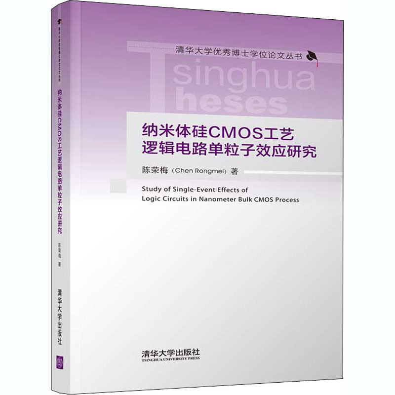
空间辐射环境对宇航电子系统构成严峻的可靠性威胁。纳米集成电路具有高性能、高集成度等优点,是未来宇航电子系统的必然选择。《纳米体硅CMOS工艺逻辑电路单粒子效应研究》深入研究纳米体硅CMOS工艺逻辑电路中单粒子效应的产生与传播受电路工作电压、频率和版图结构这些电路内在因素以及温度和总剂量两种空间环境变量的影响规律及其机理。

















评论晒单